- 您现在的位置:买卖IC网 > Sheet目录17360 > AS1339 EB (ams)BOARD EVAL AS1339
AS1339
Datasheet - A b s o l u t e M a x i m u m R a t i n g s
5 Absolute Maximum Ratings
Stresses beyond those listed in Table 2 may cause permanent damage to the device. These are stress ratings only,
and functional operation of the device at these or any other conditions beyond those indicated in Electrical Character-
istics on page 5 is not implied. Exposure to absolute maximum rating conditions for extended periods may affect
device reliability.
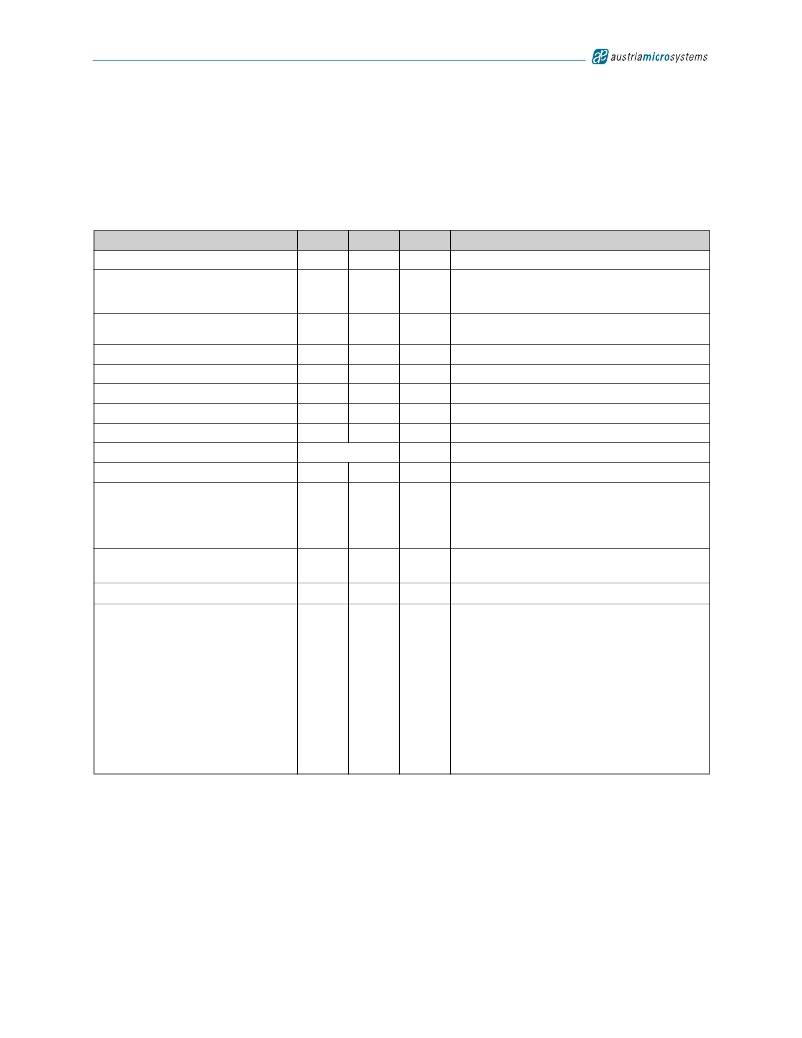
Table 2. Absolute Maximum Ratings
Parameter
IN1A, IN1B, IN2 to AGND
PAA, PAB, PA_EN, TEST, REFIN,
NC to AGND
LDO1, LDO2, EN1, EN2 to AGND
REFIN Common-Mode Range
IN2 to IN1B/IN1A
PGND to AGND
LX Current
Bypass Current
Human Body Model
Storage Temperature Range
Package Body Temperature
Min
-0.3
-0.3
-0.3
0
-0.3
-0.3
-65
1
Max
+7
V IN1A /
V IN1B +
0.3
V IN2 +
0.3
V IN
+0.3
+0.3
0.8
1.6
+150
+260
Units
V
V
V
V
V
V
A RMS
A RMS
kV
oC
oC
Comments
HBM MIL-Std. 883E 3015.7 methods
The reflow peak soldering temperature (body
temperature) specified is in accordance with
IPC/JEDEC J-STD-020D “Moisture/Reflow
Sensitivity Classification for Non-Hermetic Solid
State Surface Mount Devices”.
Continuous Power Dissipation
P D-MAX
0.75
W
T A = +65oC; derate 12.5mW/oC above +65oC
Junction Temperature (T J ) Range
-40
+125
oC
Ambient Temperature (T A ) Range
-40
+85
oC
In applications where high power dissipation
and/or poor package thermal resistance is
present, the maximum ambient temperature
may have to be derated.
Maximum ambient temperature (T A-MAX ) is
dependent on the maximum operating junction
temperature (T J-MAX-OP = 125oC), the maximum
power dissipation
of the device in the application (P D-MAX ), and the
junction-to ambient thermal resistance of the
part/package in the application ( θ JA ), as given by
the following
equation: T A-MAX = T J-MAX-OP – ( θ JA × P D-MAX ).
Revision 1.05
4 - 25
发布紧急采购,3分钟左右您将得到回复。
相关PDF资料
RB-1512S/H
CONV DC/DC 1W 15VIN 12VOUT
MIC2545A-2BM
IC SW CURR LIMIT HI SIDE 8-SOP
F971A336MCC
CAP TANT 33UF 10V 20% 2312
RB-1509S/H
CONV DC/DC 1W 15VIN 09VOUT
SB350-E3/54
DIODE SCHOTTKY 50V 3A AXIAL
MIC2505BN
IC SW SGL 2A HIGH SIDE 8-DIP
MIC2505BM TR
IC SW SGL 2A HIGH SIDE 8-SOIC
TAAB685K035G
CAP TANT 6.8UF 35V 10% AXIAL
相关代理商/技术参数
AS1339-BWLT
功能描述:IC CONV BUCK 650MA 16-WLP RoHS:是 类别:集成电路 (IC) >> PMIC - 稳压器 - 专用型 系列:- 标准包装:43 系列:- 应用:控制器,Intel VR11 输入电压:5 V ~ 12 V 输出数:1 输出电压:0.5 V ~ 1.6 V 工作温度:-40°C ~ 85°C 安装类型:表面贴装 封装/外壳:48-VFQFN 裸露焊盘 供应商设备封装:48-QFN(7x7) 包装:管件
AS1339-DB
制造商:ams 功能描述:Evaluation Board
AS1339-EB
功能描述:电源管理IC开发工具 AS1339 Evaluation Board RoHS:否 制造商:Maxim Integrated 产品:Evaluation Kits 类型:Battery Management 工具用于评估:MAX17710GB 输入电压: 输出电压:1.8 V
AS133R0HLF
制造商:TT Electronics / IRC 功能描述:AS133R0HLF
AS133R0JLF
制造商:TT Electronics / IRC 功能描述:AS133R0JLF
AS133R2FLF
制造商:TT Electronics / IRC 功能描述:AS133R2FLF
AS133R2HLF
制造商:TT Electronics / IRC 功能描述:AS133R2HLF
AS133R2JLF
制造商:TT Electronics / IRC 功能描述:AS133R2JLF
